16-bit computer on a FPGA
There are follow-ups of this topic:
- 32-bit FPGA computer,
- hardware sprites,
- the first game,
- PS/2 keyboard support,
- UART Loader,
- text mode,
- graphics mode,
- assembler,
- byte-oriented instructions.
I have made a 16-bit computer using my DE0-NANO FPGA board. The computer has 16-bit CPU, 64K 16-bit words, UART (115200 bps), and VGA (640x480, text-based frame buffer, 80x60 characters).
The Verilog code is on the github.

At first I used a breadboard

Then I have wired the board as a shield for the DE0-NANO

The schematics of the current version is above
The 16-bit CPU has 8 general-purpose registers (r0 – r7), pc (program counter), sp (stack pointer), ir (instruction register), mbr (memory buffer register), h (higher word when multiplying, or remainder when dividing).
The address bus is 16 bits wide, addressing 65536 memory
locations (words). Data bus is also 16 bits wide, having each memory location 16
bits wide. This gives 65536 16-bits words, or 128KB.
Video output is VGA, 640x480. Text mode has 80x60
characters, each character being 8x8
pixels in dimensions. Video framebuffer in text mode has 4800 16-bit
words (80x60 characters). The lower byte has the ASCII character, while the
upper byte has the attributes (3 bits for the
background color, 3 bits for the foreground color, inverted, and the last two bits unused).
It has two interrupts: IRQ0 and IRQ1. IRQ0 is connected to
the KEY2 of the DE0-NANO, while IRQ1 is connected to the UART. Whenever a byte
comes to the UART, it generates an IRQ1. Interrupt causes CPU to push flags to
the stack, then to push PC to the stack and then to jump to the location
designated for the CPU:
- for the IRQ0, it is 0x0004, and
- for the IRQ1, it is 0x0008.
It is up to the programmer to put the code in those locations.
Usually, it is a JUMP instruction. To return from the interrupt routine, it is
necessary to put the IRET instruction. It pops the return address, and then
pops the flags register, and then goes back into the interrupted program.
KEY1 of the DE0-NANO is used as the reset key. When pressed,
it forces CPU to go to the 0x0000 address. Usually there is a JUMP instruction
to go to the main program.
VGA text mode
Text mode is 80x60 characters, occupying 4800 words. Lower
byte is the ASCII code of a character, while the upper byte is the attributes:
7
|
6
|
5
|
4
|
3
|
2
|
1
|
0
|
Foreground color, inverted
|
Background color
|
||||||
r
|
g
|
b
|
r
|
g
|
b
|
||
The foreground color is inverted so zero values (default)
would mean white color. That way, you don't need to set the foreground color to
white, and by default (0, 0, 0), it is white. The default background color is
black (0, 0, 0). This means that if the upper (Attribute) byte is zero (0x00),
the background color is black, and the foreground color is white.


Attributes provide 8 foreground and 8 background colors
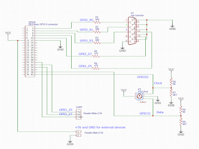
VGA female connector is connected via resistors to the
GPIO-0 expansion header of the DE0-NANO board:
- GPIO_R (pin 2, GPIO_00, PIN_A3) -> 68Ohm -> VGA_R,
- GPIO_G (pin 4, GPIO_01, PIN_C3) -> 68Ohm -> VGA_G,
- GPIO_B (pin 6, GPIO_03, PIN_D3) -> 68Ohm -> VGA_B,
- GPIO_HS (pin 8, GPIO_05, PIN_B4) -> 470Ohm -> VGA_HORIZONTAL_SYNC,
- GPIO_VS (pin 10, GPIO_07, PIN_B5) -> 470Ohm -> VGA_VERTICAL_SYNC.
UART interface
UART interface provides TTL serial communication on
115200kbps. It uses one start bit, one stop bit, and eight data bits, no
parity, no handshake.
UART is connected to the GPIO-0 expansion header of the
DE0-NANO board:
- TX (pin 32, GPIO_025, PIN_D9) should be connected to the RX pin of the PC,
- RX (pin 34, GPIO_027, PIN_E10) should be connected to the TX pin of the PC.
UART is used within the CPU via IN, and OUT instructions. RX triggers the IRQ1, which means that whenever a byte is received via UART,
the IRQ1 will be triggered, forcing CPU to jump to the 0x0008 address. There
you should place the JUMP instruction to your UART interrupt routine.
Inside the UART interrupt routine, you can get the received
byte by using the IN instruction:
in r1, [64]; r1 holds
now received byte from the UART
To send a byte, first you need to check if the UART TX is
free. You can do it by using the in instruction:
loop:
in r5, [65] ; tx busy in r5
cmp r5, 0
jz not_busy ; if not busy, send back the received
character
j loop
not_busy:
out [66], r1 ; send the character to the UART
Addresses used by the UART are in the following table:
Address
|
Description
|
64
|
Received byte from the RX part of the UART (use the IN instruction).
|
65
|
0 if the TX part of the UART is free to send a byte, 1 if TX part is
busy.
|
66
|
Byte to be sent must be placed here using the OUT instruction.
|
Assembler
The assembler for the CPU is again a fork of the customasm. This is a universal assembler, which can be used to generate machine code for any CPU. All you need is the instructions definition file. That file contains the list of instructions and the resulting machine code. For example, here are several instructions for my CPU:
#cpudef
{
#bits 16
#tokendef reg
{
r0 = 0
r1 = 1
r2 = 2
r3 = 3
r4 = 4
r5 = 5
r6 = 6
r7 = 7
sp = 8
h = 9
}
nop -> 16'0x0000
halt -> 16'0xfff0
mov {dest: reg}, {src: reg} -> src[3:0] @ dest[3:0] @ 4'0x0 @ 4'0x1
mov {dest: reg}, {value} -> 4'0x0 @ dest[3:0] @ 4'0x1 @ 4'0x1 @ value[15:0]
...
}
The assembler is on the github.
UART loader
I have hardcoded the UART loader in the RAM memory. This means that whenever I start the computer, RAM contains the loader and after the reset, the loader is started. The loader initially sends the identification sequence to the PC, and the PC then sends the program to be executed. All this is done via serial port (UART). On my PC, I use the USB-to-serial (TTL) dongle. This way, I can develop programs on my PC and then load them on the board after the reset. The protocol for the loader is a modification of the Raspbootin protocol, which I have used for my bare metal programming.
Java client for uploading images is on the github.
Java client for uploading images is on the github.
Emulator
I have made an emulator for this computer. It is written in Java and it supports full-speed execution, break points, and step-by-step execution (both step-into and step-over). It has a separate window to display characters in the VGA framebuffer, and on that window, when you press a key, it will generate an IRQ1, emulating the UART reception of a byte ("received" byte is a pressed key).
Java-based emulator is on the github.
Java-based emulator is on the github.
Conclusion
FPGA programming is fun, but also can be painful. Especially when you need to wait couple of minutes for the design to be compiled and placed on your board. Also, as I said earlier, the learning curve is very steep. You can run into a lot of problems at the beginning. First of all, you need to figure that all the lines in the Verilog are "executed" in parallel. You actually need to imagine the resulting hardware (or at least to have an idea what will be created) when programming in Verilog.
Next, you need to read warnings! Some of those warnings will actually tell you what you have done wrong in your design. I have also run into problems with the operator precedence in Verilog. I had to place brackets to make an explicit order of evaluation, because it was different from my usual experience (in other programming languages).
I used my oscilloscope extensively during the VGA signal generation and UART development. Without it I would not have been able to make them work.


Horizontal sync pulses are shown on the oscilloscope
Also, I have used the Icarus Verilog to make the simulations. It is way faster than using the Altera ModelSim tool, and much easier to work with. Unfortunately, it cannot detect timing problems, which can occur, and which can make your design fail. If that is the case, read those warnings again!
I will expand this text and write more texts about this computer and my experience with the FPGA programming.