Going 32-bit
There are follow-ups:
- implemented BLIT instruction,
- adding SPI interface to my FPGA computer,
- making BASIC interpreter for my FPGA platform,
- using GCC on my FPGA platform,
- added cache controller,
- new VGA display mode,
- booting from the SD card.
I have upgraded my FPGA-based computer from 16-bit to 32-bit. It now has 16 registers, each 32-bit. It uses 32MB SDRAM which exists on the DE0-NANO board, but it also uses static RAM for the video memory (frame buffer), for both text and graphics mode. It is approx. 40 KB of static RAM.
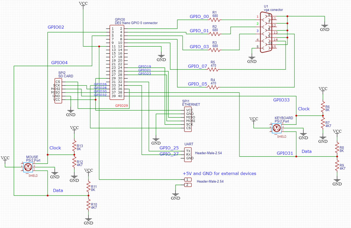
FPGA Computer Schematics
Memory management
If was quite painful to make the computer work with the SDRAM. The 32MB SDRAM needs a special controller to be used. I have found one useful controller on the github:
Since there are two types of memory in this computer (dynamic and static), I had to make a decision how to layout the memory. First 40KBs are used for the static RAM (all interrupt vectors, text and graphics video RAM and sprite definition memory). After that, the rest of the memory is in the SDRAM (up until 32MB).
If there is a need to read from the memory, this is how it is done. Let's suppose that we need to read 16 bits from the PC + 2 address:
addr <= (pc + 2) >> 1;
next_state <= EXECUTE;
state <= READ_DATA;
We need to set the next_state register to the state to which we want to return, when the read is done. Then, the CPU goes to the READ_DATA state.
READ_DATA: begin
if (addr >= SDRAM_START_ADDR) begin
waiting_sdram <= 1;
addr_o <= addr;
rd_enable_o <= 1'b1;
if (busy_i) begin
state <= READ_WAIT;
end
end
else begin
memrd <= 1'b1;
memwr <= 1'b0;
state <= READ_WAIT;
end
end
In this READ_DATA state, the CPU puts the address to the SDRAM address bus (addr_o), and sets the rd_enable to 1. Then it waits until the SDRAM is ready to read (busy_i is 1). When the SDRAM controller starts reading, the CPU goes to the READ_WAIT state.
READ_WAIT: begin
if (addr >= SDRAM_START_ADDR) begin
rd_enable_o <= 1'b0;
if (rd_ready_i) begin
waiting_sdram <= 0;
data_r <= rd_data_i;
state <= next_state;
end
end
else begin
memrd <= 1'b0;
memwr <= 1'b0;
data_r <= data;
state <= next_state;
end
end
The READ_WAIT state finishes when the data is obtained from the memory (the actual data is in the data_r register). It takes approx. 6 cycles (at 100 MHz) to fully obtain data from the memory (from READ_DATA to READ_WAIT, both to be finished). Then, the CPU goes to the next_state, as being set before this reading operation has been started.
Regarding writing to the SDRAM memory, let's suppose that we want to put something on the stack:
addr <= (regs[SP] - 2'd2) >> 1;
data_to_write <= regs[ir[11:8]][15:0];
// move sp to the next location
regs[SP] <= regs[SP] - 2'd2;
next_state <= EXECUTE;
state <= WRITE_DATA;
We need to set the next_state register to the state to which we want to return, when the write is done. Then, the CPU goes to the WRITE_DATA state.
if (addr >= SDRAM_START_ADDR) begin
waiting_sdram <= 1;
addr_o <= addr;
wr_data_o <= data_to_write;
wr_enable_o <= 1'b1;
if (busy_i)
state <= WRITE_WAIT;
end
else begin
memrd <= 1'b0;
memwr <= 1'b1;
state <= WRITE_WAIT;
end
end
In the WRITE_DATA state, the CPU would set the address to be written (addr_o), data to be written (wr_data_o), and would set the wr_enable_o to 1. Then it would wait for the controller to notify that it is ready to write (busy_i is 1). Then the CPU goes to the WRITE_WAIT state.
if (addr >= SDRAM_START_ADDR) begin
wr_enable_o <= 1'b0;
if (~busy_i) begin
waiting_sdram <= 0;
state <= next_state;
end
end
else begin
memrd <= 1'b0;
memwr <= 1'b0;
state <= next_state;
end
end
The WRITE_WAIT state finishes when the data is saved to the memory. It takes approx. 6 cycles (at 100 MHz) to fully write data to the memory (from WRITE_DATA to WRITE_WAIT, both to be finished). Then, the CPU goes to the next_state, as being set before this writing operation has been started.
CPU redesign
The CPU itself was redesigned, too. It now has quite rich instruction set, 32-bit, 16-bit and 8-bit instructions, floating point (32-bit, single precision), and three interrupts:- IRQ0 is the timer interrupt (triggered when a given number of milliseconds have been counted),
- IRQ1 is the UART interrupt (triggered when a byte has arrived), and
- IRQ2 is the PS/2 interrupt (triggered, whenever a key is pressed on the PS/2 keyboard).
The timer IRQ was made this way: there is a counter which is incremented every millisecond. There is a timer port which initially holds zero. The programmer needs to set the number of milliseconds to be counted after which the interrupt would occur. It is done using the OUT instruction:
mov.s r0, 0x0001 ; JUMP opcode
mov.s r1, TIMER_HANDLER_ADDR ; timer vector address
st.s [r1], r0
mov.w r0, timer_triggered
mov.s r1, TIMER_HANDLER_ADDR + 2
st.w [r1], r0 ; the timer IRQ handler has been set
move.w r0, 50 ; set the timer interrupt for every 50 milliseconds
out 129, r0
The assembler code above would set the internal timer register to the given value (50). Every millisecond the CPU would increase another internal register, named timer_counter, and when the timer_counter reaches the timer, that would trigger the timer interrupt:
if (timer && (timer_counter < timer)) begin
timer_counter <= timer_counter + 1'b1;
end
else if (timer && (timer_counter == timer)) begin
irq[0] <= 1;
timer_counter <= 0;
end
At the end of each instruction execution, there is a check for the interrupts:
if (irq_r[0]) begin
// timer
pc <= 16'd8;
addr <= 16'd4;
irq_r[0] <= 0;
end
If there is a timer interrupt, the CPU would jump to the TIMER_HANDLER_ADDR, which is 8.
FPGA Raspbootin loader
I have modified the FPGA Raspbootin loader so it would now load the FPGA itself, instead of relying on the Quartus II studio for that. This means that I can now control the Computer from a single application - FPGA Raspbootin:

The loader now first loads the design into the FPGA (unless it is flashed - then no loading the design file is needed), and then it loads the selected binary into the computer. Here is the Java code for loading the design into the FPGA (by starting the quartus_pgm.exe program):
public static void runFpga() {
Process process;
try {
process = new ProcessBuilder(qpfPath,
"-c", "usb-blaster",
"-m", "jtag",
"-o", "P;" + sofPath).start();
InputStream is = process.getInputStream();
InputStreamReader isr = new InputStreamReader(is);
BufferedReader br = new BufferedReader(isr);
String line;
while ((line = br.readLine()) != null) {
System.out.println(line);
}
} catch (IOException e) {
e.printStackTrace();
}
}
The qpfPath points to the quartus_pgm.exe file, which acutally loads the design into the FPGA. Usually it is something like: C:\altera\13.0\quartus\bin\quartus_pgm.exe
The design file has the *.sof extension, and it is loaded into the FPGA using the quartus_pgm.exe program. The *.sof file is built during the compilation of the design inside the Quartus II studio. In my program, the path to the *.sof file is in the sofPath variable.
More details about loading FPGA design on the DE0-NANO FPGA board can be found here:
https://mvidakovic.blogspot.com/2019/10/flashing-de0-nano-fpga-board.html
More details about loading FPGA design on the DE0-NANO FPGA board can be found here:
https://mvidakovic.blogspot.com/2019/10/flashing-de0-nano-fpga-board.html
Conclusion
The 32-bit rework took more time than I expected, mainly because I wanted to use the built-in 32MB SDRAM. Then I added the floating-point instructions and now it looks quite stable. I have used about 80% of the FPGA, so I could try to do something more later.
https://github.com/milanvidakovic/FPGAComputer32
The assembler examples are on the github:
https://github.com/milanvidakovic/Assembler32
The Raspbootin64 boot loader is on the github:
https://github.com/milanvidakovic/FPGARaspbootin64Client
The Emulator is on the github:
https://github.com/milanvidakovic/FPGAEmulator32

