Приказивање постова са ознаком computer. Прикажи све постове

петак, 6. март 2020.

Cache implemented on my FPGA computer

Introduction

This is a follow-up of my original FPGA computer post.

My FPGA computer uses SDRAM as operating memory. It has static RAM too, but most of it is used as dual-port RAM for the VGA video subsystem. The SDRAM inside is 32MB, 16-bit data bus memory and it usually takes about six clock cycles for read and the same amount of cycles for write. The clock is 100MHz. Knowing all of this, it was about time to do some performance measurement:

I have made a simple program that counts from 1 to 10 000 000. If that program is loaded in SDRAM, it takes about 15 seconds to finish. However, if I load it in static RAM, it takes about 6 seconds to finish. So, there was an obvious motivation to try to implement the cache controller. You can look at the Verilog code here:
https://github.com/milanvidakovic/FPGAComputer32/blob/master/cpu.v

Implementation

I haven't used all of the static RAM in my FPGA computer, so I was able to make about 8KB of L1 cache. Here are the details:
- I have 4096 cache lines, each having two bytes. That is 8KB of cache.
- for each cache line, I have added 12-bit TAG, used for the direct mapping of the cache line. That consumes additional 5632 bytes of static RAM.
- I have implemented write-through policy, since I didn't have enough resources to make a write-back removal policy. I will try to make write-back, but it requires a complete rework of the cache controller, so, perhaps later...

Ho this thing works in practice? First of all, here is the Verilog code:

// cache TAG
reg [11:0] tag[4095:0];
// cache line
reg [15:0] cl[4095:0];

Each cache line (a row in the cl variable) holds two bytes of data. Whenever a CPU wants to do a read, the address from the address bus goes into the cache controller:

if (tag[addr[11:0]] == addr[23:12]) begin
// cache hit (required data is in cache)
data_r <= cl[addr[11:0]];
state <= next_state;
end
else begin
// cache miss -> we need to read from SDRAM
rd_enable_o <= 1'b1;
if (busy_i) begin
state <= READ_WAIT;
end
end

12 lower bits of the address (addr[11:0]) are used to address the cache line. To check if the wanted data is in cache, the tag is used. The same 12 lower bits address the tag which is assigned to a cache line. If the upper 12 bits of the address (addr[23:12]) match those in the tag, then we have a cache hit and the data can be returned directly from the cache. 

If that is not the case, then we need to perform a read from the SDRAM, and then:

rd_enable_o <= 1'b0;
if (rd_ready_i) begin
data_r <= rd_data_i;
// we store the fetched data into the cache
cl[addr[11:0]] <= rd_data_i;
// write tag
tag[addr[11:0]] <= addr[23:12];
state <= next_state;
end

When we finally obtain the data from the SDRAM, we return that data to the CPU, but we also write down that same data in the cache line, and we update the tag associated to that cache line with the upper 12 bits of the address.

That was the read cycle. Let's see how write works. When CPU wants to write data, it is saved into the SDRAM and into the cache as well:

// Write through, meaning that we save data in both SDRAM and cache
wr_data_o <= data_to_write;
// now we need to store the data that had to be saved into cache
cl[addr[11:0]] <= data_to_write;
// write tag
tag[addr[11:0]] <= addr[23:12];
wr_enable_o <= 1'b1;
if (busy_i) begin
state <= WRITE_WAIT;
end

As we can see, data is saved in both SDRAM and cache, and then we just return back:

wr_enable_o <= 1'b0;
if (~busy_i) begin
state <= next_state;
end

Performance

The cache controller works like a charm! The same counting example works now (almost) as fast as when it was executed in the static RAM (about 6 seconds to count from 1 to 10 million). 

Conclusion

Write-through implementation is simpler than write-back and maintains SDRAM in synchronization with the cache. However, it is slower, because CPU needs to wait for the data to be saved in SDRAM, instead of doing fast save just into the cache. Write-back is faster, since we don't have to wait for the slow SDRAM save, but the cache goes out-of-sync with the SDRAM (since we saved data in cache only). When we have a full cache, in case of write-back, we need to empty the corresponding cache line, by writing the content into the SDRAM, and then to write the new content in the cache.

The write cycle could be implemented as write-back, but with this setup, I cannot do that (not enough resources on FPGA chip). I will investigate that in future.

уторак, 14. мај 2019.

32-bit FPGA-based computer

Going 32-bit

There are follow-ups:
- implemented BLIT instruction,
- adding SPI interface to my FPGA computer,
- making BASIC interpreter for my FPGA platform,
- using GCC on my FPGA platform,
- added cache controller,
- new VGA display mode,
- booting from the SD card.


I have upgraded my FPGA-based computer from 16-bit to 32-bit. It now has 16 registers, each 32-bit. It uses 32MB SDRAM which exists on the DE0-NANO board, but it also uses static RAM for the video memory (frame buffer), for both text and graphics mode. It is approx. 40 KB of static RAM.

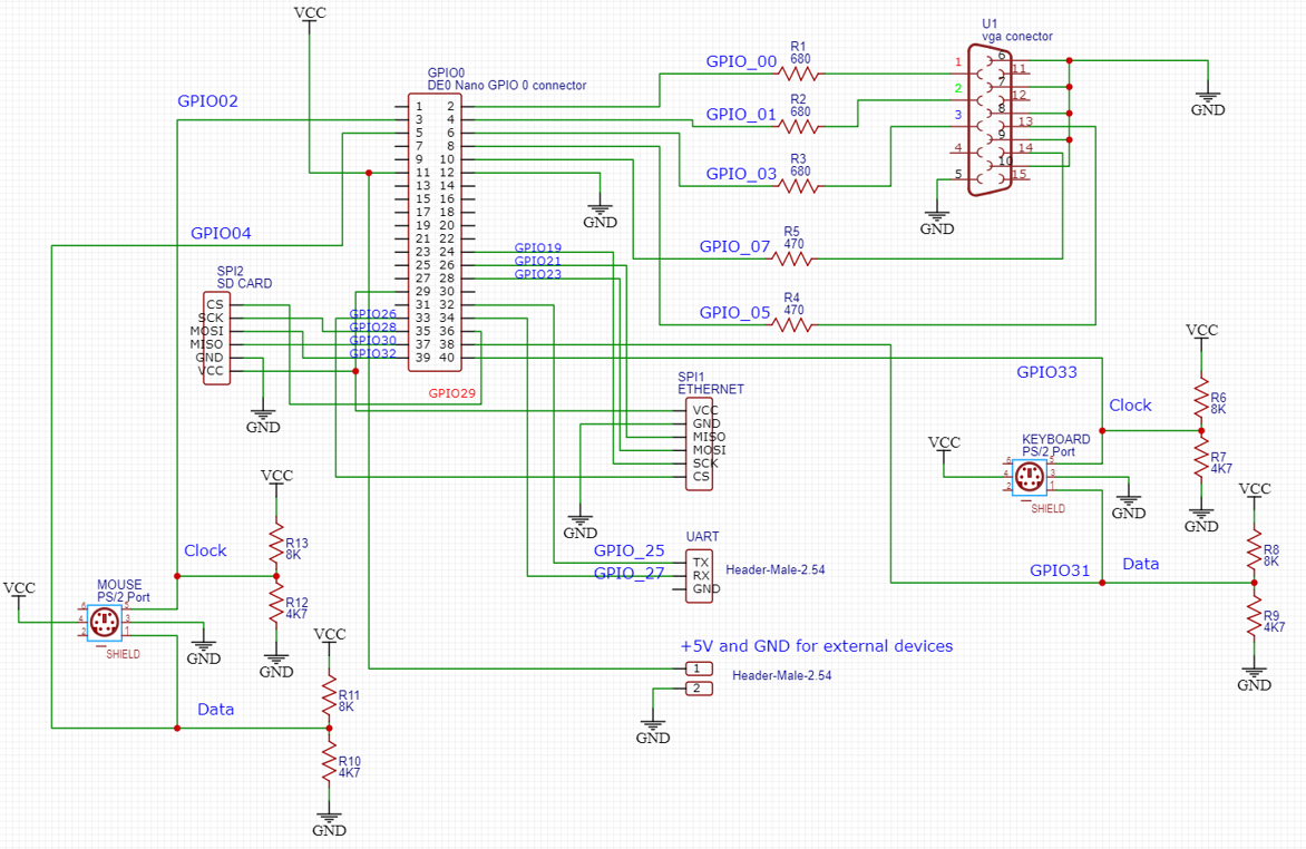
FPGA Computer Schematics

Memory management

If was quite painful to make the computer work with the SDRAM. The 32MB SDRAM needs a special controller to be used. I have found one useful controller on the github:

Since there are two types of memory in this computer (dynamic and static), I had to make a decision how to layout the memory. First 40KBs are used for the static RAM (all interrupt vectors, text and graphics video RAM and sprite definition memory). After that, the rest of the memory is in the SDRAM (up until 32MB).

If there is a need to read from the memory, this is how it is done. Let's suppose that we need to read 16 bits from the PC + 2 address:

addr <= (pc + 2) >> 1;
next_state <= EXECUTE;
state <= READ_DATA;

We need to set the next_state register to the state to which we want to return, when the read is done. Then, the CPU goes to the READ_DATA state.

READ_DATA: begin
if (addr >= SDRAM_START_ADDR) begin
waiting_sdram <= 1;
addr_o <= addr;
rd_enable_o <= 1'b1;
if (busy_i) begin
state <= READ_WAIT;
end
end
else begin
memrd <= 1'b1;
memwr <= 1'b0;
state <= READ_WAIT;
end
end

In this READ_DATA state, the CPU puts the address to the SDRAM address bus (addr_o), and sets the rd_enable to 1. Then it waits until the SDRAM is ready to read (busy_i is 1). When the SDRAM controller starts reading, the CPU goes to the READ_WAIT state. 

READ_WAIT: begin
if (addr >= SDRAM_START_ADDR) begin
rd_enable_o <= 1'b0;
if (rd_ready_i) begin
waiting_sdram <= 0;
data_r <= rd_data_i;
state <= next_state;
end
end
else begin
memrd <= 1'b0;
memwr <= 1'b0;
data_r <= data;
state <= next_state;
end
end

The READ_WAIT state finishes when the data is obtained from the memory (the actual data is in the data_r register).  It takes approx. 6 cycles (at 100 MHz) to fully obtain data from the memory (from READ_DATA to READ_WAIT, both to be finished). Then, the CPU goes to the next_state, as being set before this reading operation has been started.

Regarding writing to the SDRAM memory, let's suppose that we want to put something on the stack:

addr <= (regs[SP] - 2'd2) >> 1;
data_to_write <= regs[ir[11:8]][15:0];
// move sp to the next location
regs[SP] <= regs[SP] - 2'd2;
next_state <= EXECUTE;
state <= WRITE_DATA;

We need to set the next_state register to the state to which we want to return, when the write is done. Then, the CPU goes to the WRITE_DATA state.

WRITE_DATA: begin
if (addr >= SDRAM_START_ADDR) begin
waiting_sdram <= 1;
addr_o <= addr;
wr_data_o <= data_to_write;
wr_enable_o <= 1'b1;
if (busy_i)
state <= WRITE_WAIT;
end
else begin
memrd <= 1'b0;
memwr <= 1'b1;
state <= WRITE_WAIT;
end
end

In the WRITE_DATA state, the CPU would set the address to be written (addr_o), data to be written (wr_data_o), and would set the wr_enable_o to 1. Then it would wait for the controller to notify that it is ready to write (busy_i is 1). Then the CPU goes to the WRITE_WAIT state.

WRITE_WAIT: begin
if (addr >= SDRAM_START_ADDR) begin
wr_enable_o <= 1'b0;
if (~busy_i) begin
waiting_sdram <= 0;
state <= next_state;
end
end
else begin
memrd <= 1'b0;
memwr <= 1'b0;
state <= next_state;
end
end

The WRITE_WAIT state finishes when the data is saved to the memory.  It takes approx. 6 cycles (at 100 MHz) to fully write data to the memory (from WRITE_DATA to WRITE_WAIT, both to be finished). Then, the CPU goes to the next_state, as being set before this writing operation has been started.

CPU redesign

The CPU itself was redesigned, too. It now has quite rich instruction set, 32-bit, 16-bit and 8-bit instructions, floating point (32-bit, single precision), and three interrupts:
- IRQ0 is the timer interrupt (triggered when a given number of milliseconds have been counted),
- IRQ1 is the UART interrupt (triggered when a byte has arrived), and
- IRQ2 is the PS/2 interrupt (triggered, whenever a key is pressed on the PS/2 keyboard).

The timer IRQ was made this way: there is a counter which is incremented every millisecond. There is a timer port which initially holds zero. The programmer needs to set the number of milliseconds to be counted after which the interrupt would occur. It is done using the OUT instruction:

mov.s r0, 0x0001 ; JUMP opcode
mov.s r1, TIMER_HANDLER_ADDR ; timer vector address
st.s [r1], r0
mov.w r0, timer_triggered
mov.s r1, TIMER_HANDLER_ADDR + 2
st.w [r1], r0 ; the timer IRQ handler has been set


move.w r0, 50  ; set the timer interrupt for every 50 milliseconds
out 129, r0

The assembler code above would set the internal timer register to the given value (50). Every millisecond the CPU would increase another internal register, named timer_counter, and when the timer_counter reaches the timer, that would trigger the timer interrupt:

if (timer && (timer_counter < timer)) begin
timer_counter <= timer_counter + 1'b1;
end
else if (timer && (timer_counter == timer)) begin
irq[0] <= 1;
timer_counter <= 0;
end 

At the end of each instruction execution, there is a check for the interrupts:

if (irq_r[0]) begin
// timer
pc <= 16'd8;
addr <= 16'd4;
irq_r[0] <= 0;
end 

If there is a timer interrupt, the CPU would jump to the TIMER_HANDLER_ADDR, which is 8.

FPGA Raspbootin loader

I have modified the FPGA Raspbootin loader so it would now load the FPGA itself, instead of relying on the Quartus II studio for that. This means that I can now control the Computer from a single application - FPGA Raspbootin:


The loader now first loads the design into the FPGA (unless it is flashed - then no loading the design file is needed), and then it loads the selected binary into the computer. Here is the Java code for loading the design into the FPGA (by starting the quartus_pgm.exe program):

public static void runFpga() {
Process process;
try {
process = new ProcessBuilder(qpfPath,
"-c", "usb-blaster",
"-m", "jtag",
"-o", "P;" + sofPath).start();
InputStream is = process.getInputStream();
InputStreamReader isr = new InputStreamReader(is);
BufferedReader br = new BufferedReader(isr);
String line;
while ((line = br.readLine()) != null) {
  System.out.println(line);
}
} catch (IOException e) {
e.printStackTrace();
}
}

The qpfPath points to the quartus_pgm.exe file, which acutally loads the design into the FPGA. Usually it is something like: C:\altera\13.0\quartus\bin\quartus_pgm.exe

The design file has the *.sof extension, and it is loaded into the FPGA using the quartus_pgm.exe program. The *.sof file is built during the compilation of the design inside the Quartus II studio. In my program, the path to the *.sof file is in the sofPath variable.

More details about loading FPGA design on the DE0-NANO FPGA board can be found here:
https://mvidakovic.blogspot.com/2019/10/flashing-de0-nano-fpga-board.html

Conclusion

The 32-bit rework took more time than I expected, mainly because I wanted to use the built-in 32MB SDRAM. Then I added the floating-point instructions and now it looks quite stable. I have used about 80% of the FPGA, so I could try to do something more later.

The CPU is on the github:
https://github.com/milanvidakovic/FPGAComputer32

The assembler examples are on the github:
https://github.com/milanvidakovic/Assembler32

The Raspbootin64 boot loader is on the github:
https://github.com/milanvidakovic/FPGARaspbootin64Client

The Emulator is on the github:
https://github.com/milanvidakovic/FPGAEmulator32


субота, 24. новембар 2018.

Hardware sprites on the FPGA computer

Adding hardware sprites

This is a follow-up of the FPGA computer post. 

I have added hardware sprites to the graphic mode of my FPGA computer. It now supports up to 16 sprites, each one being 16x16pixels in size. Here is how it looks on the monitor:
In emulator, it looks the same:


Each sprite is defined by the 8-byte structure:
  • sprite definition data address (2 bytes)
  • x coordinate (2 bytes)
  • y coordinate (2 bytes)
  • transparent color (2 bytes).
The sprite structure for the first sprite starts at address of 56 decimal. Each next sprite structure starts 8 bytes later. 

Sprite definition data consists of 16 lines, each line described by 16 pixels, each pixel defined by 4 bits: xrgbThis means that one sprite line consists of 8 bytes (two pixels per byte), so total bytes needed for the sprite definition is 8x16 bytes == 128 bytes.

Here is the example of showing one sprite at (25, 25) in assembler language:

  mov r0, sprite_def
  mov r1, 56
  st [r1], r0  ; sprite definition is at sprite_def address
  mov r0, 25
  st [r1 + 2], r0  ; x = 25  at addr 58
  mov r0, 25
  st [r1 + 4], r0  ; y = 25  at addr 60
  mov r0, 0
  st [r1 + 6], r0  ; transparent color is black (0) at addr 62
  ; sprite definition
sprite_def:
  #d16 0x0000, 0x0000, 0x0000, 0x0000  ; 0
  #d16 0x0000, 0x000f, 0xf000, 0x0000  ; 1
  #d16 0x0000, 0x000f, 0xf000, 0x0000  ; 2
  #d16 0x0000, 0x000f, 0xf000, 0x0000  ; 3
  #d16 0x0000, 0x004f, 0xf400, 0x0000  ; 4
  #d16 0x0000, 0x004f, 0xf400, 0x0000  ; 5
  #d16 0x0000, 0x044f, 0xf440, 0x0000  ; 6
  #d16 0x0000, 0x444f, 0xf444, 0x0000  ; 7
  #d16 0x0004, 0x444f, 0xf444, 0x4000  ; 8
  #d16 0x0044, 0x444f, 0xf444, 0x4400  ; 9
  #d16 0x0400, 0x004f, 0xf400, 0x0040  ; 10
  #d16 0x0000, 0x004f, 0xf400, 0x0000  ; 11
  #d16 0x0000, 0x004f, 0xf400, 0x0000  ; 12
  #d16 0x0000, 0x041f, 0xf140, 0x0000  ; 13
  #d16 0x0000, 0x4111, 0x1114, 0x0000  ; 14
  #d16 0x0004, 0x4444, 0x4444, 0x4000  ; 15

How this stuff works? First of all, I had to decide how to implement sprites. I have decided to fetch all sprite data during the vertical blanking interval (VBI). During VBI, the video subsystem starts fetching sprite data by reading the 8-byte sprite structure starting from the address of 56 decimal (the address and data bus are 16-bit, so the computer is word-oriented (reads two bytes at the same time), and the actual address is set to
56 >> 1 == 28):

if ((x >= 640) && (y == 479) && (state == IN_LINE)) begin
  // when we start the vertical blanking, 
  // we need to fetch in advance the first sprite data
  state <= READ_SPRITES;
  sprite_counter <= 4'b0;
  rd <= 1'b1;
  wr <= 1'b0;
  mem_read <= 1'b1;
  addr <= 16'd28;    // prepare to read sprite definition address
end

In the next clock cycle, the system is in the READ_SPRITES state. The first thing that we do in the READ_SPRITES state is fetching the sprite definition address which is present at the data bus, since we have initiated a memory read from within the previous state.

Then we need to prepare the address bus for the next state in which we will fetch the x coordinate of the sprite. We do that by setting the address bus to (58 + (sprite_counter << 3)) for all sprites, having the sprite_counter iterating from 0 to 15:

READ_SPRITES: begin
  sprite_addr[sprite_counter] <= data;
  state <= READ_SPRITE_X;
  rd <= 1'b1;
  wr <= 1'b0;
  mem_read <= 1'b1;
  // prepare to read x coordinate of the sprite
  addr <= (16'd58 + (sprite_counter << 3)) >> 1;    
end

In the READ_SPRITE_X state, we fetch the x coordinate of the sprite which was ready at the data bus, and then we prepare to read the y coordinate in the next state:

READ_SPRITE_Y: begin
  sprite_y[sprite_counter] <= data;
  state <= READ_SPRITE_TRANSPARENT_COLOR;
  rd <= 1'b1;
  wr <= 1'b0;
  mem_read <= 1'b1;
  // prepare to read transparent color of the sprite  
  addr <= (16'd62 + (sprite_counter << 3)) >> 1;    
end

In the READ_SPRITE_Y state, we fetch the y coordinate of the sprite which was ready at the data bus, and then we prepare to read the sprite transparent color in the next state:

READ_SPRITE_TRANSPARENT_COLOR: begin
  sprite_transparent_color[sprite_counter] <= data[3:0];
  state <= READ_SPRITE_DATA;
  rd <= 1'b1;
  wr <= 1'b0;
  mem_read <= 1'b1;
  line_counter <= 16'b0;
  word_counter <= 4'b0;
  // read sprite definition bytes
  addr <= sprite_addr[sprite_counter] >> 1;    
end

In the READ_SPRITE_TRANSPARENT_COLOR state, we fetch the transparent color of the sprite, and then put the address of the sprite definition to the address bus so we can fetch it in the next state:

READ_SPRITE_DATA: begin
  if (line_counter < 16) begin
    case (word_counter) 
    0:  sprite_pixels[sprite_counter][line_counter][63:48] <= data;
    1:  sprite_pixels[sprite_counter][line_counter][47:32] <= data;
    2:  sprite_pixels[sprite_counter][line_counter][31:16] <= data;
    3:  sprite_pixels[sprite_counter][line_counter][15:0]  <= data;
    endcase
    state <= READ_SPRITE_DATA;
    rd <= 1'b1;
    wr <= 1'b0;
    mem_read <= 1'b1;
    if (word_counter < 3) begin
      word_counter = word_counter + 1'b1;
    end
    else begin
      word_counter = 1'b0;
      line_counter = line_counter + 16'b1;
    end
    // read sprite definition bytes
    addr = (sprite_addr[sprite_counter] + ((word_counter +
           (line_counter << 2)) << 1) ) >> 1;    
  end
  else 
  begin
    if (sprite_counter < SPRITE_NUM) begin
      sprite_counter = sprite_counter + 1'b1;
      state <= READ_SPRITES;
      rd <= 1'b1;
      wr <= 1'b0;
      mem_read <= 1'b1;
      // read next sprite definition address
      addr <= (16'd56 + (sprite_counter << 3)) >> 1;   
    end
    else begin
      sprite_counter <= 4'b0;
      rd <= 1'b1;
      wr <= 1'b0;
      mem_read <= 1'b1;
      addr <= VIDEO_MEM_ADDR + 0;
      state <= V_BLANK;
    end
  end
end

In the READ_SPRITE_DATA state we start reading sprite definition from the memory. We do it for each line of the sprite (16 lines per sprite), and within the line, for each word containing four pixels of the sprite line definition.

When we finish loading all sprite definition data for the current sprite, then we do the same for other sprite until we read all sprite definition data. Then we then set the address bus to load the pixel data at the (0, 0) position on the screen, and move to the V_BLANK state:

V_BLANK: begin
  pixels <= data;
  state <= SCAN_IDLE;
  rd <= 1'bz;
  wr <= 1'bz;
  mem_read <= 1'b0;
end

In the V_BLANK state we read the pixels of the frame buffer at the (0, 0) coordinate, and then set the all the control signals to high impedance and set the state to SCAN_IDLE. We will leave the SCAN_IDLE state when the the time comes to start displaying pixels starting from the (0, 0) coordinate.

Displaying sprite data

During the scanline processing, we need to display both original pixels from the frame buffer as well as the sprite data, and we need to make sure that the original pixels must be displayed through the transparent sprite color.

This is done in the following code:

if (valid) begin
  for (i = 0; i < SPRITE_NUM; i = i+1) begin
    if ((sprite_addr[i] != 16'b0) &&
       (xx >= sprite_x[i]) &&
       (xx < (sprite_x[i] + 16)) &&
       (yy >= sprite_y[i]) &&
       (yy < (sprite_y[i] + 16))) begin

      sprite_found = 1'b1;
      if (
        sprite_pixels[i][yy - sprite_y[i]][60-(((xx - sprite_x[i]) << 2) ) + 0] != sprite_transparent_color[i][0] ||
        sprite_pixels[i][yy - sprite_y[i]][60-(((xx - sprite_x[i]) << 2) ) + 1] != sprite_transparent_color[i][1] ||
        sprite_pixels[i][yy - sprite_y[i]][60-(((xx - sprite_x[i]) << 2) ) + 2] != sprite_transparent_color[i][2]
      ) begin
        r <= sprite_pixels[i][yy - sprite_y[i]][60-(((xx - sprite_x[i]) << 2) ) + 0] == 1'b1;
        g <= sprite_pixels[i][yy - sprite_y[i]][60-(((xx - sprite_x[i]) << 2) ) + 1] == 1'b1;
        b <= sprite_pixels[i][yy - sprite_y[i]][60-(((xx - sprite_x[i]) << 2) ) + 2] == 1'b1;
      end 
      else begin
        r <= pixels[12 - ((xx & 3) << 2) + 0] == 1'b1;
        g <= pixels[12 - ((xx & 3) << 2) + 1] == 1'b1;
        b <= pixels[12 - ((xx & 3) << 2) + 2] == 1'b1;
      end
    end 
  end
  if (!sprite_found) begin
    r <= pixels[12 - ((xx & 3) << 2) + 0] == 1'b1;
    g <= pixels[12 - ((xx & 3) << 2) + 1] == 1'b1;
    b <= pixels[12 - ((xx & 3) << 2) + 2] == 1'b1;
  end
  else begin
    sprite_found = 1'b0;
  end
end
else begin
  // blanking -> no pixels
  r <= 1'b0;
  g <= 1'b0;
  b <= 1'b0;
end
end

The most interesting thing is the "for loop". It is not a loop - it actually repeats the Verilog code SPRITE_NUM times. That is the most important thing to understand about "loops". You don't have the linear code to be executed multiple times. Instead, everything is a giant state machine that pulses with the clock signals and the "for loop" just unwraps the code multiple times, and all that unwrapped code "works" at the same time.

So, when we have this Verilog code:
 for (i = 0; i < SPRITE_NUM; i = i+1) begin
    if ((sprite_addr[i] != 16'b0) &&
       (xx >= sprite_x[i]) &&
       (xx < (sprite_x[i] + 16)) &&
       (yy >= sprite_y[i]) &&
       (yy < (sprite_y[i] + 16))) begin

It actually does this:
    if ((sprite_addr[0] != 16'b0) &&
       (xx >= sprite_x[0]) &&
       (xx < (sprite_x[0] + 16)) &&
       (yy >= sprite_y[0]) &&
       (yy < (sprite_y[0] + 16))) begin

...
    end
    if ((sprite_addr[1] != 16'b0) &&
       (xx >= sprite_x[1]) && 
       (xx < (sprite_x[1] + 16)) && 
       (yy >= sprite_y[1]) && 
       (yy < (sprite_y[1] + 16))) begin
...
    end
...


The code with the "for loop" does the same thing for all sprites:
  1. if the spite definition address is not zero, and current x and y coordinates of the scanline are within sprite coordinates, then we put the current sprite pixel color to the output r, g and b signals, or we put the original frame buffer pixel colors, if the current sprite pixel is transparent one (the color of the current sprite pixel is the transparent color).
  2. else, if the current x and y coordinates of the scanline are outside of the sprite coordinates, we put the frame buffer pixel data to the r, g and b output signals.
  3. else, it must be blanking interval, so put zeros to r, g and b to output signals.

Conclusion

This implementation of sprites requires that the vga module has its own internal memory which is filled with the sprite data from the main memory. Then, during the scanline processing, sprite pixels are combined with frame buffer pixels in a way that sprite pixels are placed "over" the frame buffer pixels, unless the current sprite pixel is the transparent one. If that is the case, then the frame buffer pixel is "shown" through the sprite.

The great thing about hardware sprites is that they do not consume processor time at all. Everything is done in hardware and showing sprites actually requires just to have the sprite definition address set to non-zero value.

петак, 7. септембар 2018.

Snakes!

The first game on my FPGA platform

This is a follow-up of the FPGA computer post. 

I have decided to make a game for the FPGA Computer. My friend gave me his Pascal implementation of the Snakes game and I have ported it into the FPGA Assembler. Not an easy task, but it works now:


The game was made to work in the video text mode. The frame is constructed using '-', '+', and '|' characters. The head of the snake is '@', the body is 'O', the star is '*', and when the snake hits the wall or its tail, we get the 'X' character at the crash scene.

In the emulator it works the same way:

The game is placed on the github.

Milliseconds counter register

During the game development, it occured to me that I need to implement the milliseconds counter register in order to implement the delay function. In the cpu.v file, I have created two additional registers:

reg [N-1:0] millis_counter;

reg [15:0] clock_counter;


The millis_counter register will hold the number of milliseconds counted so far. Incrementing this register is done whenever clock_counter reaches 50000 (clock is 50MHz, which means that when the clock_counter reaches 50000, one millisecond has elapsed):

always @ (posedge CLOCK_50) begin
if (clock_counter < 50000) begin
clock_counter <= clock_counter + 1'b1;
end
else begin
clock_counter <= 0;
millis_counter <= millis_counter + 1'b1;
end
...

To read the millis_counter register, I have introduced another port address for the IN instruction:

4'b0011: begin
  // IN reg, [xx]
  `ifdef DEBUG
  $display("%2x: IN r%-d, [%4d]",ir[3:0], (ir[11:8]), data);
  `endif
  case (mc_count)
0: begin
mbr <= data;  // remember the address of IO port
mc_count <= 1;
pc <= pc + 2'd2;  // move to the next instruction
end
1: begin
    case (mbr)
64: begin    // UART RX DATA
regs[ir[11:8]] <= {8'b0, rx_data_r};
end
65: begin   // UART TX BUSY
regs[ir[11:8]] <= tx_busy;
end
68: begin    // keyboard data
regs[ir[11:8]] <= {8'b0, ps2_data_r};
end
69: begin // milliseconds counted so far
regs[ir[11:8]] <= millis_counter;
end
  endcase // end of case(mbr)
  ir <= 0;      // initiate fetch
  addr <= pc >> 1;
end
default: begin
end
  endcase  // end of case (mc_count)
end // end of IN reg, [xx]

The example of the usage can be found in the snakes.asm file:

; ################################################################
; function delay(r0)
; waits for the r0 milliseconds
; ################################################################
delay:
push r1
push r2
delay_loop2:
in r1, [PORT_MILLIS] ; port 69
delay_loop1:
in r2, [PORT_MILLIS] ; port 69
sub r2, r1
jz delay_loop1 ; one millisecond elapsed here
dec r0
jnz delay_loop2
pop r2
pop r1
ret

Conclusion

This was the first game made for the FPGA Computer. The game is quite simple and uses video text mode. I had to implement a milliseconds counter register and the corresponding IN port to read it. It was used to implement the delay function. 


четвртак, 30. август 2018.

PS/2 keyboard and FPGA Computer

Added PS/2 keyboard to the FPGA Computer

This is a follow-up of the FPGA computer post. 

I have added a keyboard port to the FPGA Computer. The port is PS/2 because it is easier to work with the PS/2 than with the USB HID protocol. The final look is here (you will recognize the purple PS/2 keyboard connector):

The hardware part of this project is simple - add four resistors and a PS/2 connector:
Now the board has three connectors: PS/2, VGA and UART.

PS/2 connector is connected to the GPIO ports of the DE0-NANO board:
- Data is connected to the GPIO31 (PIN_D11) port
- Clock is connected to the GPIO33 (PIN_B12) port.

The communication between keyboard and computer is a clocked serial. Clock pulses appear on the Clock pin, while data is on the Data pin, synchronized with the Clock on the falling edge. There is one start bit, one parity bit and one stop bit. Here are oscilloscope snapshots of the "A" key being pressed (and then released):

The waveform below is the make code of the "A" key (1C hex)


The waveform below is the first byte of the "A" break code (F0 hex)

The waveform below is the second byte of the "A" break code (1C hex)

Keyboards work by sending the make and the break codes for each key. Make code is sent when the key is pressed, while the break code is sent when the key is released. For example, when we press and then release the "A" key, we get the following sequence:
1C F0 1C
This could be interpreted as: A pressed (1C), A released (F0 1C)

Unfortunately, it is all not that simple. First of all, if you quickly press A and C, one after another, you will get the following sequence:
1C 1B F0 1B F0 1C
This could be interpreted as: make code of "A", make code of "S", break code of "S" and break code of "A".

When you press Shift + A, you will get the following sequence:
12 1C F0 1C F0 12
Shift pressed, A pressed, A released, Shift released

When you press A for a long time (autorepeat will occur):
1C 1C 1C 1C 1C F0 1C
A pressed, A pressed, A pressed, A pressed, A pressed, A released (F0 1C)

To make things more complicated, extended key codes (both make and break) have been introduced, for some keys. For example, the Cursor Down (Arrow Down) key produces the following sequence:
E0 72 E0 F0 72
Cursor down pressed (E0 72), Cursor down released (E0 F0 72).

And so on... All this makes parsing a bit complicated, but eventually you will be able to figure it out.

The next step was to add the support for the keyboard within the FPGA Computer.

Introducing the keyboard interrupt

I have introduced a new interrupt for the keyboard - the IRQ#2. This IRQ is triggered when a byte from PS/2 keyboard arrives. The CPU then jumps to the address of 24 decimal, where the raw PS/2 keyboard handling routine should be. Actually, at that address should be one JUMP instruction which will jump to the handling routine.

In the main computer module, I have instantiated the PS/2 module:
// ####################################
// PS/2 keyboard instance
// ####################################
wire [7:0] ps2_data;
wire ps2_received;
reg [7:0] ps2_data_r;

ps2_read ps2(
  CLOCK_50,
  reset,
  gpio0[31], // Input pin - PS/2 data line
  gpio0[33], // Input pin - PS/2 clock line
  ps2_data,  // here we will receive a character
  ps2_received  // if something came from PS/2, this goes high
); 

Then I have detected the byte being received from the PS/2 module and triggered the IRQ:


always @ (posedge CLOCK_50) begin
// ######### IRQ2 - keyboard ######
if (ps2_received) begin
ps2_data_r <= ps2_data;
// if we have received a byte from 
// the keyboard, we will trigger the IRQ#2
irq[2] <= 1'b1;
end 
...


In the cpu.v module, I have added a support for the new interrupt:
if (irq_r[2]) begin
`ifdef DEBUG
LED[7] <= 1;
$display("3.1 JUMP TO IRQ #2 SERVICE");
`endif
pc <= 16'd24;
addr <= 16'd12;
end

So, to receive bytes from the PS/2 keyboard, a programmer must register the IRQ#2 handler:
; set the IRQ handler for keyboard to our own IRQ handler
mov r0, 1 ; JUMP instruction opcode
mov r1, IRQ2_ADDR ; IRQ#2 vector address
st [r1], r0
mov r0, irq_triggered
mov r1, IRQ2_ADDR + 2   
st [r1], r0

Since this is raw PS/2 handling, the programmer must write the complete make/break code handling. I have done that in this example.

Unfortunately, the code is quite long since it has to deal with the raw PS/2 protocol. The code demonstrates parsing the raw PS/2 protocol and it looks like those vintage screen editors:

How to use the keyboard? First of all, two callbacks should be registered - one for the key pressed, and the other one for the key released:
mov r0, 1 ; JUMP instruction opcode
mov r1, KEY_PRESSED_HANDLER_ADDR
st [r1], r0
mov r0, pressed ; key pressed routine address
mov r1, KEY_PRESSED_HANDLER_ADDR + 2
st [r1], r0

mov r0, 1 ; JUMP instruction opcode
mov r1, KEY_RELEASED_HANDLER_ADDR
st [r1], r0
mov r0, released ; key released routine address
mov r1, KEY_RELEASED_HANDLER_ADDR + 2
st [r1], r0

Both callbacks will then need to obtain the virtual key code of the key pressed (or released) by reading from the location 48 (VIRTUAL_KEY_ADDR):

pressed:
ld r0, [VIRTUAL_KEY_ADDR]
cmp r0, VK_F1
...

released:
ld r1, [VIRTUAL_KEY_ADDR]
...

What is the Virtual Key Code? It is a number assigned to each key, so all the programs would get the same number when a key is pressed, or released. In the code above, VK_F1 is the constant assigned to the F1 key, so the programmer can determine if the F1 was pressed by writing cmp r0, VK_F1.

Then, if needed, programmer can call the vk_to_char function which translates a virtual key to  the actual character, if possible (not all keys produce characters; F1 key does not produce character, for example):

; ###############################
; r1 = function vk_to_char(r1)
; translates virtual key to character
; if shift is pressed, does the uppercase
; ###############################
vk_to_char:
push r0
push r2
...

Conclusion

Most examples for keyboard support on the net use PS/2 keyboards, since USB HID protocol is quite complex and PS/2 isn't. I went the same path. I have couple of spare keyboards, some of them are PS/2, so I have soldered the PS/2 female connector and those four resistors from the schematics above. From that point on, everything was programming - a little bit of Verilog programming, and much more of assembler programming.